How PCB Flex Circuits Can Be Used in IoT Devices
PCB Flex Circuits Can Be Used in IoT Devices
The Internet of Things, or IoT, has revolutionized our world. It is bringing smart, wearable devices with enhanced functionality and superior mechanical characteristics into our daily lives. This has prompted an industry shift in PCB manufacturing that is leveraging the power of flexible concepts. These are called flex circuits, and they help to create small, compact IoT devices that can meet the needs of even the most demanding designers.
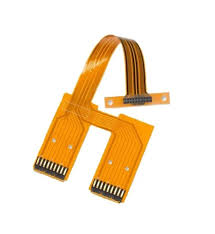
Unlike traditional rigid boards, pcb flex are made of thin substrates that offer high levels of bending and tensile strength, making them ideal for IoT devices. They also eliminate the need for external wire harnesses that would require additional assembly, soldering, and wrapping. This simplifies the design process and reduces overall production costs.
These thin boards can be molded into complex shapes and feature multiple layers to house various electronic components. As such, they are highly versatile and are used in a variety of applications including fitness trackers, medical devices, and cameras. They are also able to withstand harsh environments, making them ideal for use in outdoor equipment and military-grade technology.
How PCB Flex Circuits Can Be Used in IoT Devices
There are several different types of flex PCBs, but the most popular are single-sided and double-sided boards. Both are made of a base layer, conductive metal layer, protective solder mask, and silk screen. The latter is often used as a visual indicator to identify the different layers of the flex board. It can be a valuable tool in the early stages of a flex PCB design and allows designers to experiment with the placement of their components.
It is important to design a flex circuit with the right copper layer size for the intended application. Using too much copper can result in the trace cracking under the stress of repeated bending and can negatively impact performance. To avoid this, a thinner conductive copper layer is recommended. Additionally, a design with rounded corners is more resistant to bending than one with sharp corners.
A flex circuit’s copper layer is attached to the substrate with an adhesive or special base material. This method was once problematic because it reduced the flex circuit’s reliability, but manufacturers have developed adhesiveless PI that attaches directly to the copper, eliminating the need for an adhesive. This is a significant improvement in the reliability of flex circuits and makes them more attractive for use in IoT devices.
Several considerations must be taken into account when designing a flex PCB, including the bend radius, bend ratio, and strains created at different locations on the flex circuit. It is also crucial to place vias appropriately and ensure they can withstand the stresses of bending and curvature. A good rule of thumb is to leave at least 20 mils between the via and other layers. This allows the via to “bounce” around the surface of the flex circuit, and it can help to reduce via fatigue and failure. Lastly, it is critical to test the flex circuit for durability before production.